Semiconductor Devices: Diodes, Transistors, and Their Applications
The Science of Semiconductor Devices
Author: Geetha Editorial Team
Published: Nov 11, 2025
Last Updated: Feb 13, 2026
Semiconductor devices are the foundation of modern electronics, enabling everything from smartphones to power systems. Semiconductors are materials with electrical properties between conductors and insulators. By precisely controlling their properties, engineers create devices with remarkable capabilities. Understanding semiconductor devices—particularly diodes and transistors—is fundamental to understanding modern electronics and electrical engineering.
Semiconductor Fundamentals
Pure semiconductors like silicon and germanium have four valence electrons. At room temperature, they have limited conductivity. However, by adding impurities (doping), we dramatically alter their properties:
N-type (Negative) Semiconductor: Created by adding donors (impurities with 5 valence electrons, like phosphorus). Extra electrons become free charge carriers. Electrons are the majority carriers.
P-type (Positive) Semiconductor: Created by adding acceptors (impurities with 3 valence electrons, like boron). Missing electrons create holes that act as positive charge carriers. Holes are the majority carriers.
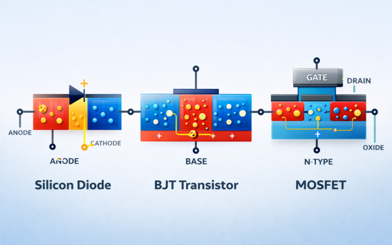
The PN junction, where p-type and n-type materials meet, is the basis for most semiconductor devices.
Diodes: The Simplest Semiconductor Device
A diode is the simplest semiconductor device, consisting of a single PN junction. It allows current flow easily in one direction (forward bias) but blocks it in the other (reverse bias).
Forward Bias: Positive voltage applied to p-region and negative to n-region. This reduces the potential barrier, allowing charge carriers to flow easily. Forward current exponentially increases with voltage above the threshold voltage (about 0.6V for silicon).
Reverse Bias: Opposite voltage applied. This strengthens the barrier, preventing current flow. Ideally, reverse current is zero, though in practice, tiny leakage currents flow.
Breakdown: At sufficiently high reverse voltage, the junction breaks down and conducts in reverse. Some diodes, like Zener diodes, are designed to operate in this breakdown region.
Diode Applications: Rectification (converting AC to DC), voltage regulation (Zener diodes), signal detection, frequency multiplication, and protection (clamping and clipping circuits).
Special Diodes:
Light Emitting Diodes (LEDs) emit light when forward biased. Energy released as charge carriers recombine produces photons. LEDs are highly efficient light sources, transforming lighting and display industries.
Photodiodes generate current when illuminated. They’re used in light detection, camera sensors, and fiber-optic communications.
Tunnel diodes exhibit negative resistance regions, used in specialized high-frequency applications.
Schottky diodes use a metal-semiconductor junction instead of PN junction, having lower forward voltage and faster switching speeds.
Transistors: The Amplifying Device
Transistors are three-terminal devices that can amplify signals and switch currents. They form the basis of all digital and analog electronics. Two main types exist: bipolar junction transistors (BJTs) and field-effect transistors (FETs).
Bipolar Junction Transistors (BJTs): BJTs consist of two PN junctions creating a sandwich structure: either NPN or PNP. The three terminals are collector, base, and emitter.
In NPN transistors, small base current controls large collector current. The current gain (β or hFE) determines how much the collector current exceeds the base current, typically 50-300 for modern transistors.
BJTs operate in three regions: cutoff (no conduction), saturation (maximum conduction), and active region (intermediate conduction with current gain). The active region is used for amplification, while saturation and cutoff are used for switching applications.
Field-Effect Transistors (FETs): FETs control current flow using an electric field applied to the gate terminal. Because gate current is essentially zero, FETs are voltage-controlled devices with extremely high input impedance.
Junction FETs (JFETs) use reverse-biased PN junctions to control the channel. Metal-Oxide-Semiconductor FETs (MOSFETs) use an insulated gate, enabling even higher impedance.
MOSFETs dominate modern electronics because they’re easy to manufacture in integrated circuits, have minimal power consumption, and can be made extremely small.
Transistor Applications
Amplification: BJTs and FETs amplify weak signals. Different configurations (common emitter, common source, etc.) provide different gain and impedance characteristics. Analog electronics uses carefully biased transistors in linear regions.
Switching: Transistors switch between on and off states, controlling power delivery or digital signal routing. Digital electronics is built on switching transistors.
Logic Gates: CMOS (complementary metal-oxide-semiconductor) technology uses complementary pairs of MOSFETs to create logic gates with minimal power consumption.
Power Electronics: Specialized power transistors handle high currents and voltages, controlling motors, power supplies, and industrial equipment.
Transistor Characteristics and Ratings
Important specifications include:
Maximum Ratings: Absolute maximum voltages, currents, and power dissipation that cannot be exceeded without damage.
Gain (β or hFE): Collector current divided by base current for BJTs; determines amplification.
Transconductance (gm): For FETs, the change in output current divided by change in input voltage.
Frequency Response: How transistor amplification changes with signal frequency. Parasitic capacitances limit high-frequency performance.
Noise Figure: Added noise from the transistor. Important in sensitive applications like radio receivers.
Integrated Circuits
Modern electronics use integrated circuits (ICs) containing thousands to billions of transistors. From simple gates to complex microprocessors, all use transistor principles scaled down to nanometer dimensions.
Scaling Benefits: Smaller transistors switch faster, consume less power, and cost less to manufacture. However, scaling introduces challenges: parasitic effects, heat dissipation, and quantum effects become significant.
Moore’s Law: Historically, transistor counts doubled every two years. While this trend is slowing, it enabled exponential growth in computing capability for decades.
Semiconductor Technology Trends
Current challenges include heat dissipation in high-performance processors, power efficiency (critical for mobile devices), and reaching physical limits of silicon scaling. Emerging technologies include:
3D integrated circuits stacking transistors vertically for higher density. Gallium Nitride (GaN) and Silicon Carbide (SiC) for high-power and high-frequency applications. Tunnel FETs and other novel devices exploring alternatives to MOSFETs. Flexible electronics on plastic substrates for wearable applications.
Silicon (Si) IGBT vs. Silicon Carbide (SiC) MOSFET Comparison
| Characteristic | Si IGBT | SiC MOSFET |
|---|---|---|
| Forward Voltage Drop | 0.8-2.0V | 0.5-1.5V |
| Switching Frequency | 1-20 kHz typical | 10-100+ kHz typical |
| Conduction Loss | Higher at high frequencies | Lower across range |
| Efficiency | 93-96% | 97-99% |
| Cost | ~-5 per unit | ~-20 per unit |
| Thermal Management | More cooling required | Less cooling required |
| Best Applications | Cost-sensitive, lower frequency | High efficiency, high-frequency |
Worked Examples
Example 1: Forward Bias Current Calculation
Problem: A silicon diode has V_f = 0.7V forward voltage. What current flows when 5V is applied across a 470Ω resistor in series with the diode?
Solution:
Given: V_applied = 5V, V_f = 0.7V, R = 470Ω
Voltage across resistor: V_R = V_applied – V_f = 5 – 0.7 = 4.3V
Using Ohm’s Law: I = V_R/R = 4.3/470 = 9.15 mA
Verification: Reasonable for a typical small-signal diode.
Example 2: BJT Collector Current
Problem: A BJT has β (current gain) = 100 and base current I_B = 50µA. Calculate collector current.
Solution:
Given: β = 100, I_B = 50µA
Using relationship: I_C = β × I_B
I_C = 100 × 50µA = 5 mA
Interpretation: A small base current of 50µA is amplified to 5mA collector current.
Example 3: Transistor Power Dissipation
Problem: A BJT operates at V_CE = 2V and I_C = 100mA. Calculate power dissipated in the transistor.
Solution:
Given: V_CE = 2V, I_C = 100mA = 0.1A
Power: P = V_CE × I_C = 2 × 0.1 = 0.2 watts = 200 mW
Thermal consideration: Requires a heat sink if continuous operation to prevent overheating.
Key Takeaways
- Semiconductors are materials with controlled conductivity—silicon and germanium form the basis of modern electronics.
- Doping (adding impurities) creates N-type and P-type materials—forming the PN junction that is fundamental to all semiconductor devices.
- Diodes are the simplest semiconductor devices—conducting in forward bias, blocking in reverse bias, essential for rectification and switching.
- BJTs (Bipolar Junction Transistors) are current-controlled devices—used for amplification and switching with three terminals (Base, Collector, Emitter).
- FETs (Field Effect Transistors) are voltage-controlled—including JFETs and MOSFETs, widely used in modern integrated circuits and power electronics.
- Emerging wide-bandgap devices (SiC, GaN) enable higher efficiency and faster switching in power electronics applications.
- Device selection depends on application requirements—considering frequency, power, cost, and thermal characteristics.
Leave a Reply